

Flexible, Affordable Electronics Education
Online courses and webinars for the printed circuit engineering community.
Current Workshops
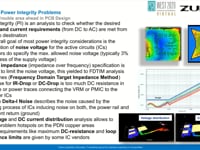
From DC to AC - Power Integrity and Decoupling Primer for PCB Designers
Supply voltages decrease with every new silicon generation, contributing as well to the goal of reducing power consumption of our electronics. Coupled with the resulting shrinking noise margins for... [more]

Best DFM Practices for Board Engineers
There is more to board design than placing parts and connecting the signals electrically. Those who design the board can make a huge impact on the ease of fabrication and assembly just by adhering... [more]

PCB Design Techniques to Improve ESD Robustness
Raise the shields, Scotty! Starting with some simple definitions for ESD/EOS, this session describes the important differences in the energy involved and the type of damage that can result. The... [more]
The 5 Ws of Flex Circuits
The 5 Ws of Flex Circuits is a breakdown of the basics of flexible circuits: What is flex? Why use flex? Who should know flex? When to use flex Where to use flex Presenter Ata Syed is... [more]
Topics


