

Flexible, Affordable Electronics Education
Online courses and webinars for the printed circuit engineering community.
Current Workshops
PCB Design and Assembly Process Strategy for High Density CSP, WLP, 2D and 3D Semiconductor Package Technology
Topics covered: 1. BGA/CSP process technologies and standards; single die BGA and FBGA packaging, flip-chip and die-size package technologies, wafer level packaging (WLP), fan-out wafer-level... [more]
Power Delivery System Design
With the advent of ICs with multiple power rails at very high currents, the design of the power delivery system in a modern product is often more difficult than routing the PCB to ensure good signal... [more]
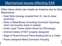
Mechanical Design to Control EMI
As most engineers and designers are aware, EMI occurs because some mechanical structure, within or attached to our system, is capable of resonating and radiating electromagnetic field energy. Those... [more]
Manufacturing by Design is the New DfM
Today’s SMT and PTH assembly processes are driven by component packaging technology and functional design requirements. These requirements are driving manufacturing/test toward “build right” and... [more]
Topics


