

Flexible, Affordable Electronics Education
Online courses and webinars for the printed circuit engineering community.
Current Workshops
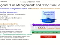
The New SEMI SMT-ELS Standards Suite for SMT and PCBA Lines
With an estimated 80,000 SMTP lines in use standards are a lifeline for line operators and equipment and software developers worldwide. SEMI is developing a suite of standards for SMT and PCBA... [more]
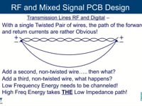
RF and Mixed Signal PCB Layout
This session is intended for board designers to understand the things RF engineers request during PCB layout. Experienced RF engineers will likely not learn anything new from this course, as the... [more]
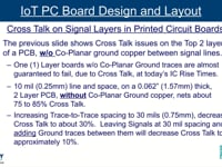
IoT PC Board Design and Layout
Circuit boards for the IoT world (Internet of Things) are often driven by the need for low power dissipation, low cost (which drives very low layer count), moderate to high-density and mixed-signal... [more]

How to Fight Magnetic Noise Gremlins
Have you ever had a noise-sensitive circuit and tried to find the noise source? Even after you completely encased sensitive portions in all sorts of shielding, you still had noise? It’s very... [more]
Topics


